== 概要 ==
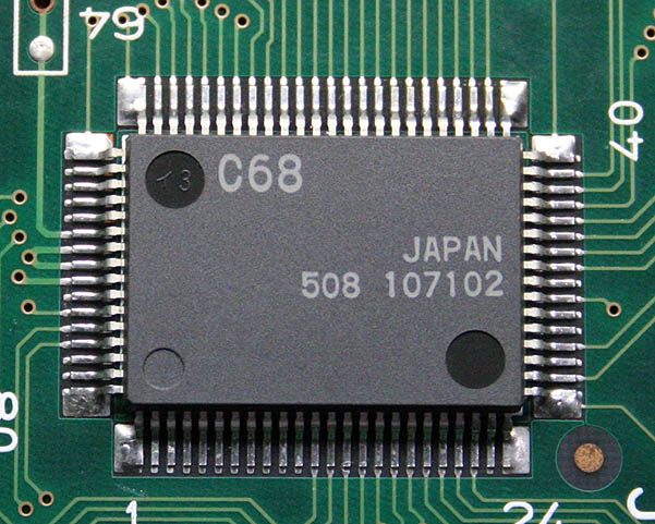
C68(CUS68)はナムコ
SYSTEM IIメイン基板二代目に搭載されているLSI。入出力制御用のワンチップマイコン。
== 外観 ==
== 仕様 ==
- C68(CUS68)
- パッケージ 80ピンQFP
- 電源電圧
When I was working on the C69 MCU found in the Namco NA-1 hardware, it came to my attention that later Namco System 2 boards had a C68 MCU instead of the HD63705 which earlier revisions used. It seemed reasonable to assume Namco used a M37702 as well considering the C68 and C69 are physically identical. I had picked up two Suzuka 8 Hours boards to examine the C68 and see what possibilities there were for trojaning it.
The MCU interface is virtually unchanged for the C68 compared to the previous System 2 boards, except for some slightly different connections and a new address decoding PAL. However the C68 pinout doesn't match any of the M377xx series. After disassembling some of the external program ROM dumps used by the C68 in a few games, investigation of the code shows it's actually a Mitsubishi 740 series based MCU, which is a 6502 core with extra instructions and features. Of course when Mitsubishi's microprocessor division was transferred to Renesas, they dropped support (and documentation!) of the older chips. I was able to reverse engineer the PAL outputs to put together the original equations and come up with a memory map, as well as make a partial pinout of the C68.
However, I need some help locating a datasheet (user manual) for it, and I don't know the official part number. The C68 is a 100-pin QFP plastic chip, rectangular in shape with pin counts of 24, 16, 24, and 16 pins going around the perimeter from pin 1. The part has a date marking of 1991. While there are many modern parts that are similar to this chip, most of them are for USB or LED segment drivers and do not have an external address/data bus, which the C68 does. The 3806 group of the 740 series, particularly the M38063M6-XXXFP seems like a very close match, but the pins are shifted around. I already have the 740 software manual (e740sum.pdf).
Feature-wise, it has eight analog channels, possibly 6 or more I/O ports (going by Mitsubishi's nomenclature, ports 0,1,2 are the data, address low, address high buses, and ports 3,4,5 are used for general I/O), internal RAM of at 256 to 512 bytes at $0000-007F/$0100-013F, and internal mask ROM of an unknown size. Another unusual feature is that the SFRs are at $D0-$FF instead of $00-$3F which may help in identifying it. In the following pinout, the address/data buses, CNVss, and analog converter channel inputs have to match whatever chip is being looked at as a potential candidate, the others are not critical. I've been through everything I can find at the Renesas website and in my collection of manuals, so I'm fairly sure the C68 corresponds to a part that is no longer in production or supported.
If anyone has any tips or ideas about which chip this part is based on, I'd certainly like to hear your suggestions!
C68 pinout:
| Pin |
|
| 1 |
??? |
| 2 |
I/O port; IK1 pin 7 |
| 3 |
I/O port; IK1 pin 9 |
| 4 |
I/O port; 1P/2P mux input group IF3 1Y |
| 5 |
I/O port; 1P/2P mux input group IF3 4Y |
| 6 |
I/O port; 1P/2P mux input group IF3 2Y |
| 7 |
I/O port; 1P/2P mux input group IF3 3Y |
| 8 |
I/O port; 1P/2P mux input group IJ3 1Y |
| 9 |
I/O port; 1P/2P mux input group IJ3 4Y |
| 10 |
I/O port; 1P/2P mux input group IJ3 2Y |
| 11 |
I/O port; 1P/2P mux input group IJ3 3Y |
| 12 |
I/O port; GOUT2 |
| 13 |
I/O port; GOUT1 |
| 14 |
I/O port; GOUT0 |
| 15 |
I/O port; COIN1 (was PA6) |
| 16 |
I/O port; COIN2 (was PA5) |
| 17 |
To PAL pin 3 |
| 18 |
I/O port; LOCK (was PA3) |
| 19 |
I/O port; !VBLANK (was PA1) |
| 20 |
To PAL pin 6, 2F pin 1 (DIR on RD7-0 bus which was IOR|W) |
| 21 |
To PAL pin 5 |
| 22 |
To PAL pin 4 (and 2C C149 pin 27, was IOR|W) |
| 23 |
|
| 24 |
|
| 25 |
CNVss (To JP18.2) |
| 26 |
/RESET (!SUBRES) |
| 27 |
|
| 28 |
CLK input (8 MHz, same as 2A p11) |
| 29 |
|
| 30 |
??? |
| 31 |
To PAL pin 2 |
| 32 |
GND (Vss) |
| 33 |
CPU D7 |
| 34 |
CPU D6 |
| 35 |
CPU D5 |
| 36 |
CPU D4 |
| 37 |
CPU D3 |
| 38 |
CPU D2 |
| 39 |
CPU D1 |
| 40 |
CPU D0 |
| 41 |
??? |
| 42 |
CPU A15 (To PAL pin 7) |
| 43 |
CPU A14 |
| 44 |
CPU A13 |
| 45 |
CPU A12 |
| 46 |
CPU A11 |
| 47 |
CPU A10 |
| 48 |
CPU A9 |
| 49 |
CPU A8 |
| 50 |
CPU A7 |
| 51 |
CPU A6 |
| 52 |
CPU A5 |
| 53 |
CPU A4 |
| 54 |
CPU A3 |
| 55 |
CPU A2 |
| 56 |
CPU A1 |
| 57 |
CPU A0 |
| 58 |
A-D channel ?/8 input (from C16) |
| 59 |
A-D channel ?/8 input (from C17) |
| 60 |
A-D channel ?/8 input (from C18) |
| 61 |
A-D channel ?/8 input (from C19) |
| 62 |
A-D channel ?/8 input (from C20) |
| 63 |
A-D channel ?/8 input (from C21) |
| 64 |
A-D channel ?/8 input (from C22) |
| 65 |
A-D channel ?/8 input (from C23) |
| 66 |
|
| 67 |
|
| 68 |
|
| 69 |
+5V (Vcc) |
| 70 |
GND (Vss) (through filter) |
| 71 |
+5V (Vcc) |
| 72 |
+5V (Vcc) |
| 73 |
GND (Vss) |
| 74 |
I/O port; Group IF3/IJ3 mux select output |
| 75 |
I/O port; RSCLK (was PC2) |
| 76 |
I/O port; SCOUT (was PC0) |
| 77 |
I/O port; Input from optocoupler using SCINA/SCINK (was PC1) |
| 78 |
I/O port; IK1 pin 3 |
| 79 |
I/O port; IK1 pin 5 |
| 80 |
??? |
I'm looking forward to writing code for the C68 as I've been wanting to work with the 740 series chips for a while now. And hopefully, a method to read the internal ROM can be figured out.
== その他 ==
== リンク ==
== 外部リンク ==
最終更新:2013年03月18日 09:49